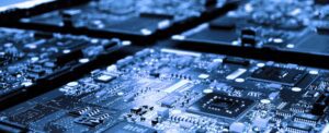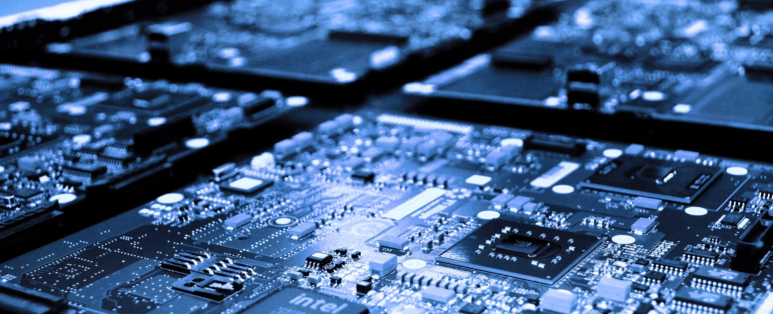
Electrical elements are becoming a significant part of our daily lives. Everything is running from smartphones to vehicles just because of the printed circuit board or short form known as PCB units. People know that the printed circuit boards are the major electrical part for which most items are running. These small green coloured units, covered with lines and copper parts help run the machines with full efficiency.
Additionally, these circuit boards are created with fibreglass, copper lines and other metal parts. These boards are connected with an insulated solder mask. Also, the solder mask is the main reason which results in the green colour.
Working of the circuit board and its component
Boards which are stuck solidly and in use for decoration of PCB boards only. As an advanced circuit board, it won’t work as its functionality until the components are completely mounted over it. PCBs mount over the assembled PCB, and the manufacturing process is widely known as PCB assembly. The copper lines on which the bare board is called trace, electrically link and components with each other. In some major parts of the world, PCB assembly California is done.
The PCB assembly California has a very simple process that consists of several automated and manual steps. With every step in this process, board manufacturers have manual and automatic options to choose from.
Learn PCB Design
The PCB process always starts with the most basic unit, i.e. the base. It consists of different layers, and it plays a significant role in functionality. There are some other alternate layers which include:
Substrate
A substrate is the base material of the PCB unit which makes PCB rigid. It is responsible for holding the different components of the PCB. Therefore, choosing the right type of substrate is considered to be one of the most fundamental steps in making a high quality PCB.
Copper
A foil with a very thin layer of conductive copper, is added to each functional side on the PCB, in which one side is PCB and on the other one is Double-side PCB.
Solder mask
Solder mask is the top copper layer that gives PCB, and due to solder, it turns to green colour. It adds the copper trace from contact with conductive materials. Holes present over the solder mask are where the soldier is in application to attach components for the board. With a solder mask, it is a vital step for making the board smooth.
Silkscreen
white silk screen provides the final layer on the PCB board. It adds a layer over the PCB in the form of different characters.
PCB Assembly process
Surface mount technology
It is a sensitive component with very small elements like resistors or diodes, which are placed automatically on the board’s surface. This is known as SMD assembly for surface mount devices. Surface mount technology can be applicable to small size components. Solder paste is applicable to the board with the help of a solder printer. A template is in use to ensure that the solder can be accurate. This is left with correct places where every component is mounted, known as a stencil.
Thru-hole technology
It works well on the lead and wire components that are mounted after plugging into the through-holes. The extra lead part is soldered on the other side. Some major boards carry the thru-hole components, which requires the high technology of thru-hole. With PCB assembly California every part comes as the best unit.
To learn about the latest technology trends and updates visit https://our-articles.com/